1.Equipment Front End Module (EFEM)
1.Introduction to EFEM
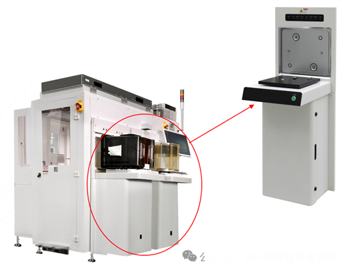
EFEM (Equipment Front End Module) is a key subsystem in semiconductor manufacturing equipment, mainly used for automated wafer transfer and microenvironment control. It is located at the front end of process equipment such as etching machines, thin film deposition equipment, etc., serving as a "bridge" for the entry and exit of wafers into the process chamber, ensuring that the wafers are not contaminated during transportation, while improving production efficiency and automation level.
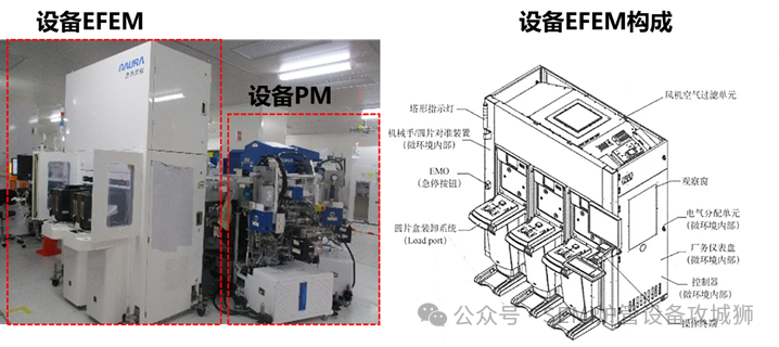
2.EFEM structure and function
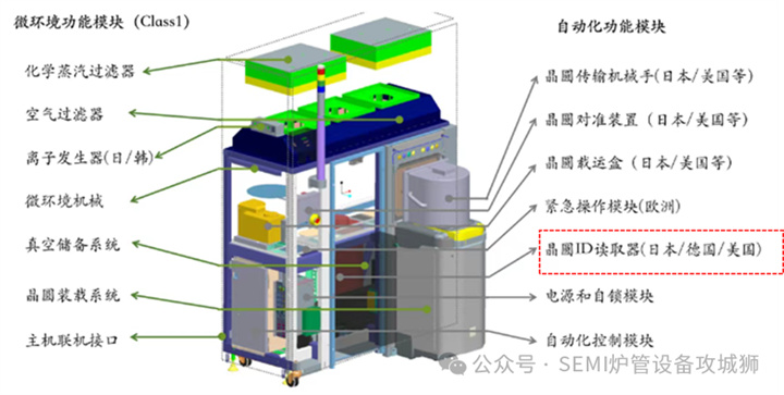
The internal structure and system of EFEM (Equipment Front End Module) are mainly divided into three major modules: Microenvironment Function Module, Automation Function Module, and Software Module.
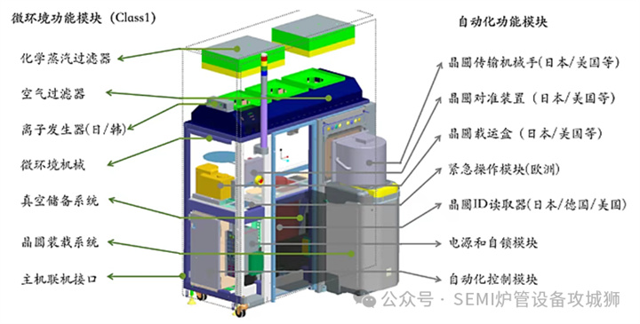
(1) Microenvironment module
Function::
Provide a high cleanliness local environment to ensure that the wafer is not contaminated by external factors during transportation.Maintain stable temperature, humidity, and particle size levels through high-efficiency filters (HEPA/ULPA) and airflow control (vertical laminar or negative pressure design).
Key components:
• Mini Environment: Closed structure with built-in sensors to monitor particles, temperature and humidity.
• FFU (Fan Filter Unit): Provides filtered clean airflow.
• Nitrogen purge function: optional configuration, used for oxygen sensitive processes.
(2) Automation functional module
Function::
Realize precise and high-speed handling of wafers between carriers (such as FOUPs) and process chambers.
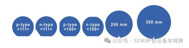
Supports multiple wafer sizes (such as 200mm/300mm) and various carrier types.
Key components:
• Robot: A multi axis robotic arm (such as SCARA or 6-axis robots) equipped with an end effector to grip wafers. High precision positioning (within ± 0.1mm) and anti-collision design.
• Load Port: Docked with FOUP/FOSB, supports automatic door opening and wafer mapping.
• Aligner: Calibrate the position and angle of the wafer (Notch/Orientation).
• Buffer Station: Temporary storage of wafers to optimize transfer efficiency.
(3)Software module
Function::
Control hardware actions (such as robot path planning, vehicle communication).
Integrate with the upper level system of the factory (MES/EAP) to achieve production data management and fault diagnosis.
Key subsystems:• SECS/GEM communication: Compliant with SEMI standards, exchanges wafer processing instructions and status information with the host system.
• Motion control software: robotic arm trajectory optimization, anti shake algorithm, fault recovery logic.
• Wafer Tracking: Identify wafer IDs through RFID or barcode and record transmission history.
• Diagnosis and logging: Real time monitoring of equipment status, generating alarms and maintenance reports.
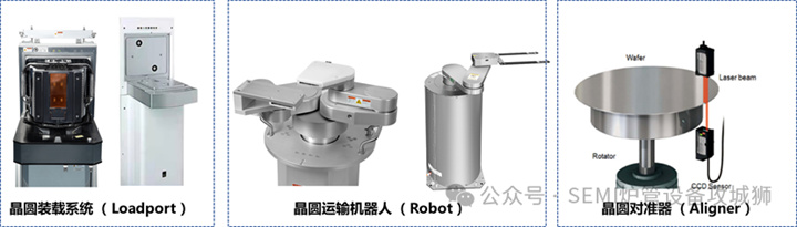
2.Wafer loading system (load port)
1.Load port structure
Load Port is a key component of EFEM (Equipment Front End Module), mainly used for docking wafer carriers (such as FOUP/FOSB) to achieve automated wafer transfer.
Load ports generally have 1-4 loading areas, which can accommodate 1-4 Foups at the same time. The specific quantity can be customized.
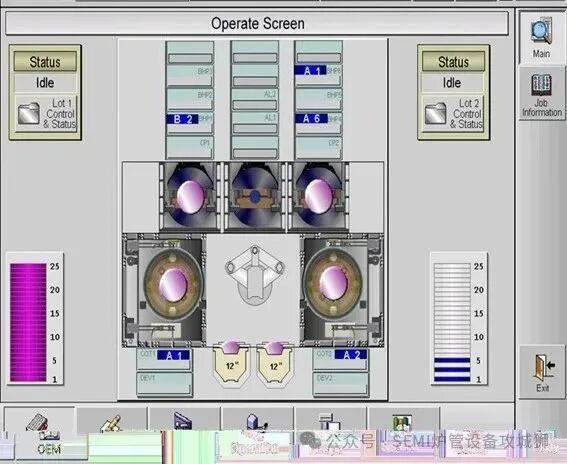
The specific steps for loading and unloading wafer boxes on the load port are as follows: OHT or manual handling of the wafer box to the loading platform → locking of the wafer box by the clamping mechanism on the loading platform → suction or clamping of the wafer box door by the opening device → separation of the wafer box door from the wafer box → movement of the detection mechanism in the vertical direction and scanning of the wafers inside the box → transportation of the wafers by the transport robot → merging of the wafer box door and the wafer box by the opening device after the wafers inside the box are transported → unlocking of the wafer box by the clamping mechanism → OHT or manual removal of the wafer box.
The entire process will be demonstrated through real-time animation on the computer side of the machine. Any problem with any step will trigger an equipment alarm and pause some transmission mechanical actions, waiting for engineers to handle it. Common alarms include Foup box door opening/closing failure, detection of protruding wafers or abnormal stacking, mismatch between the number of wafers in the material box and MES system, Foup ID recognition failure, and so on.
2. Load port function (fully automated equipment)
Equipped with RFID function, it can automatically identify the Foup box's ID and display it in real-time on the computer;
The mounting standard meets the SEMI E63 standard.
Equipped with a pressure detection sensor to check for any deviation in the Foup position.
The platform height standard (FOUP/FOSB Load Height) complies with SEMI E1.5/E63.
Compliant with the E84 standard for semiconductors, supporting OHT/mobile robot handling.
Compliant with SECS/GEM, TCP/IP and other protocols.
It has automatic door opening/closing function, wafer quantity and box position, and wafer protrusion detection function. When there is an abnormality, the mechanical action stops and an alarm is triggered.
During the process of returning the wafer to the material box after the wafer process is completed, it is necessary to ensure that there is no phenomenon of oblique insertion or wrong slot insertion, and the wafer cannot collide with objects such as the wafer rack.
The load port has good sealing to prevent wafer contamination caused by poor airtightness.
Support N2 purge to ensure that the Foup is in N2 state, preventing wafer contamination and oxidation.
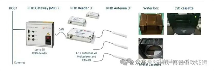
3.How to read Foup ID from load port
Implant RFID tags on each FOUP box, which record the information of the wafer and have a unique ID code inside the RFID tag. RFID readers at different manufacturing equipment are used to identify RFID tags, understand the current completion progress of the tags, check the corresponding workflow entered into different RFID tags, and verify and inspect them with the control system to confirm and proceed to the next processing step.
As shown in the figure below, it is a schematic diagram of the principle of RFID module recognizing Foup ID. After placing Foup on the load port, the infrared sensing module on the device will recognize the Foup RFID tag. Through the RFID read-write module, the tag information, namely Foup ID, will be recognized; After identifying the Foup ID, the information is transmitted to the device host and MES system through the EAP system.
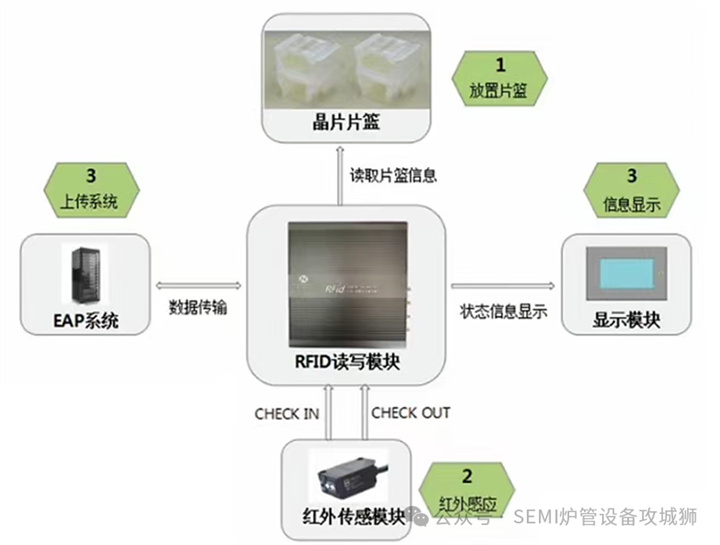
Working principle of RFID
Location of ID reader in Loadport
4.How to identify Foup on a load port
1. Mechanical contact detection (limit switch/micro switch)
Principle:
Install mechanical limit switches in the vehicle placement area of the load port. When the FOUP is placed in place, the switch is triggered and a signal is sent to the control system.
Advantages:
• Simple structure and low cost
• Strong anti-interference ability
Disadvantages:
• Mechanical wear and limited lifespan
• Accurate positioning is required, otherwise it may trigger incorrectly
• Applicable scenarios:
• Early equipment or low-cost solutions
2. Photoelectric sensor (non-contact detection)
(Mainstream method, commonly used for 300mm FOUP)
Detection method
• Reflective photoelectric sensor: emits infrared light to detect the reflected signal at the bottom of FOUP. If the reflected light is received, it indicates the presence of FOUP.
• Contrastive photoelectric sensor: emits light at one end and receives it at the other end, triggering a signal when FOUP is obstructed.
Advantages:
• Non contact, no mechanical wear and tear
• Fast response (millisecond level)
• Can detect whether FOUP is fully placed in place
Disadvantages:
• Possible interference from ambient light (anti-interference model needs to be selected)
• Dust or pollution may affect detection
Industry standards:
SEMI E15/E19 (FOUP size standardization to ensure sensor compatibility)
3. Pressure sensor (weighing detection)
Principle:
Load Port countertop integrated pressure sensor/weighing module. When FOUP is placed, a weight change triggers a detection signal.
Advantages:
• Can detect empty/full load FOUP (to prevent overweight or abnormalities)
• Not affected by optical pollution
Disadvantages:
• relatively high cost
• Regular calibration is required
Applicable scenarios:
High end equipment that needs to detect FOUP weight
4. RFID/barcode verification (secondary verification)
Principle:
After detecting the physical presence of FOUP, further confirm the identity of the vehicle through RFID or barcode scanning. If the ID cannot be read, it may be determined as an invalid FOUP.
Advantages:
• Improve safety and prevent incorrect vehicles from entering
• Integrate with MES system to achieve full automation
Disadvantages:
• Relying on additional recognition systems
5. Vacuum adsorption detection (used in a few devices)
Principle:
The load port table has vacuum adsorption holes, which form a seal after placing the FOUP. The vacuum pressure sensor detects whether the adsorption is successful and confirms the presence of FOUP.
Advantages:
• High reliability, suitable for harsh environments
Disadvantages:
• Complex structure and high maintenance cost
3.Wafer transfer robot
1.Robot Introduction
A semiconductor robot is one of the important components of semiconductor equipment, usually composed of controllers, drivers, arms, and end effectors. It has the characteristics of high cleanliness, high stability, high precision, high efficiency, and high reliability. Semiconductor robotic arms are mainly used in the front-end processes of semiconductor manufacturing, for transporting, transporting, and positioning semiconductor wafers.
2.Robot classification
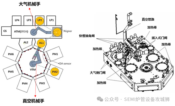
(1) Application environment classification (atmospheric manipulator and vacuum manipulator)
Semiconductor robotic arms are mainly divided into two categories based on their application environment: atmospheric robotic arms and vacuum robotic arms. Atmospheric robotic arms are mainly used for wafer transfer in atmospheric pressure environments such as coating, developing, photolithography, furnace tubes, and wet processes. They use light metal materials, servo motors, and harmonic reducers to achieve high-speed and smooth operation, with the characteristics of low cost and easy maintenance, occupying more than 60% of the market share. Vacuum robotic arms are used in vacuum environments such as PVD, etching, CVD, etc. They achieve efficient transmission through direct drive motors, vacuum isolation, and precision servo control. The material requirements are extremely strict, including preventing gas evaporation, withstanding high temperature radiation, and controlling particle pollution. Although the cost is high, it can ensure the stability of the vacuum environment and process accuracy. There are significant differences between the two types of robotic arms in terms of material selection, driving methods, and environmental adaptability, which jointly meet the automation needs of different process links in semiconductor manufacturing.
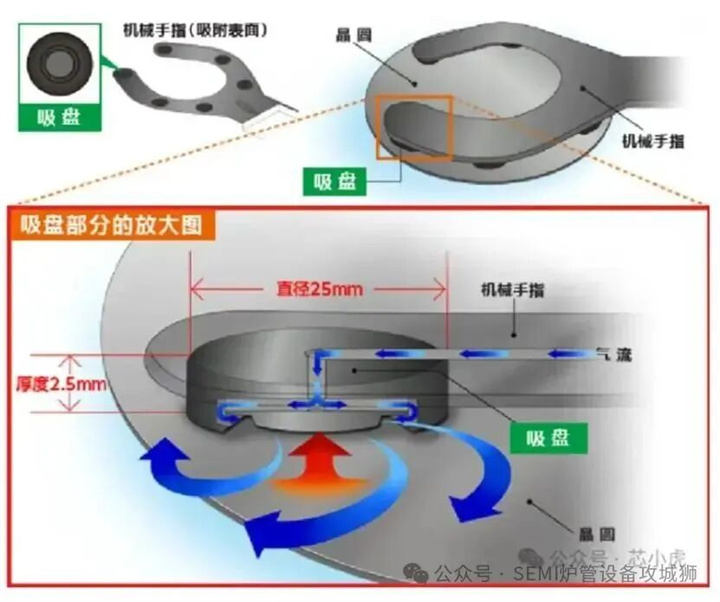
(2) The way the robotic arm holds the wafer (vacuum adsorption, mechanical clamping, Bernoulli robotic arm)
Vacuum adsorption stabilizes the suction of wafer surface through negative pressure principle, suitable for leveling wafers without causing mechanical stress.
Mechanical clamping uses a precise edge clamping mechanism to directly fix the outer edge of the wafer, which is suitable for special process requirements but poses a risk of contact contamination.
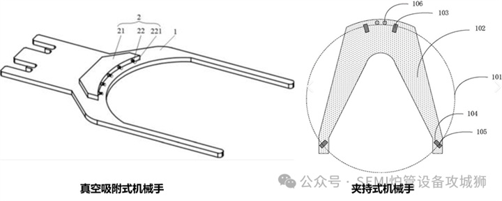
The Bernoulli robotic arm utilizes the principle of aerodynamics to form a non-contact suspension support, which creates a low-pressure area below the wafer through airflow for contactless handling. It is particularly suitable for ultra clean environments and fragile wafer transportation, completely avoiding pollution or damage caused by physical contact.
These three methods have their own characteristics and meet the transmission needs of different process environments and wafer types. Among them, vacuum adsorption is the most widely used, while Bernoulli robotic arms are mainly used in advanced processes that require extremely high cleanliness.
3.Material classification of robotic arms (alumina ceramic robotic arms, silicon carbide ceramic robotic arms)
In semiconductor equipment, the materials commonly used for robots are mainly divided into two categories: alumina ceramics and silicon carbide ceramics, each with its own unique advantages and disadvantages.
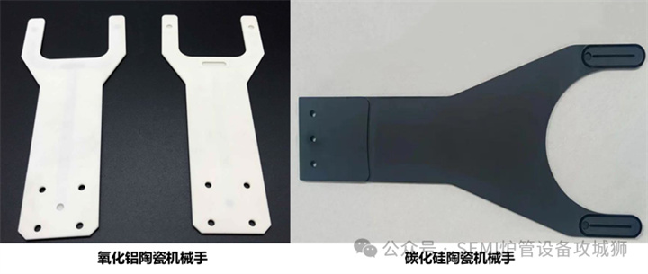
Advantages of alumina ceramic robotic arm
• High strength and hardness: The higher the purity of alumina ceramics, the smaller the size; The higher the strength, the more suitable it is for mechanical handling of semiconductor equipment. Good electrical insulation performance: alumina ceramics have a resistivity of up to 10 ^ 15 Ω· cm at room temperature and an insulation strength of up to 15 kV/mm.
• Excellent heat resistance: melting point up to 2050 ℃, not easily deformed during semiconductor heat treatment, suitable for high-precision operation.
• Good chemical stability: Alumina ceramics have stable chemical properties and will not contaminate semiconductor components.
• Mature processing technology and high cost-effectiveness: Alumina ceramic materials are easy to obtain, with relatively low prices and mature processing technology.
Disadvantages of alumina ceramic manipulator
Compared to other high-performance materials, silicon carbide ceramics may not perform as well in extreme environments such as higher temperatures or corrosive environments.
Advantages of silicon carbide ceramic robotic arm
• High strength and hardness: Silicon carbide ceramics have extremely high strength and hardness, and excellent wear resistance.
• Excellent thermal conductivity: Silicon carbide ceramics have high thermal conductivity and are suitable for applications that require heat dissipation.
• Lightweight: Compared to alumina, silicon carbide ceramics have a lower density and are lighter in weight.
Disadvantages of silicon carbide ceramic robotic arm
• Processing difficulty: Compared with alumina, the processing difficulty and cost of silicon carbide ceramics are higher.
• High price: Due to its excellent performance and processing difficulty, the price of silicon carbide ceramics is usually higher than that of alumina ceramics.
In summary, alumina ceramic robotic arms are more commonly used in semiconductor equipment due to their excellent cost-effectiveness, while silicon carbide ceramic robotic arms are suitable for applications that require extreme performance. The choice of material for the robotic arm needs to be considered based on specific application requirements and budget.
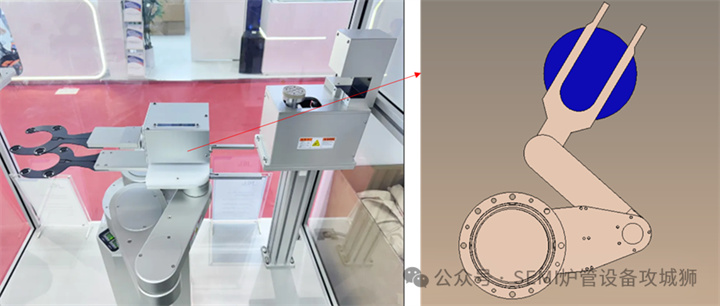
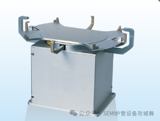
4.Wafer edge finder(Aligner)
1.The Function and Function of Aligner
Wafer flat and notch are important features used in the wafer manufacturing process to determine wafer orientation, and they play a crucial role in wafer processing, alignment, and inspection.
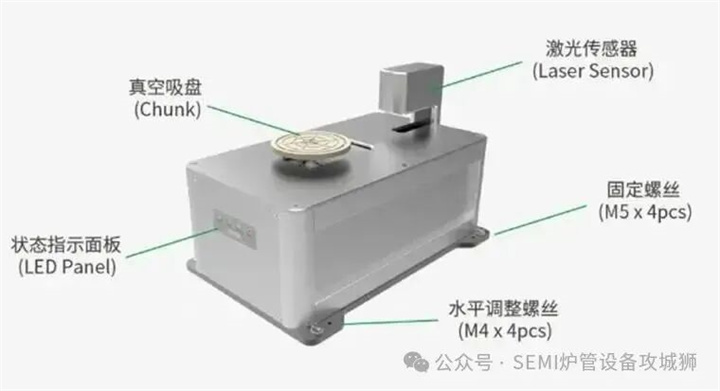
The wafer aligner in semiconductor equipment EFEM is used for wafer positioning and alignment. It is the core component of EFEM and can accurately perform wafer center core positioning and angle correction. The wafer position is ≤± 0.1mm, and the wafer edge/gap is ≤± 0.1 °.
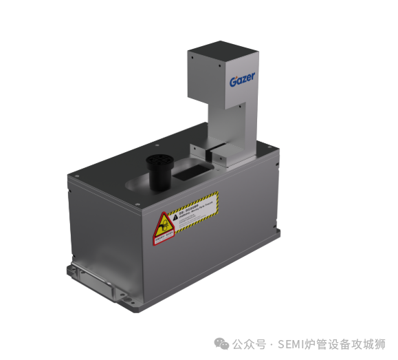
The main functions of a wafer aligner are twofold: one is to locate the center of the wafer, and the other is to find edges (angle correction).
Why do we need to do wafer center positioning? Due to the displacement of the wafer in the Foup during transportation, it is difficult to ensure that the wafer is in the center of the robotic arm when held. Therefore, an aligner is needed for wafer center positioning to ensure that the wafer center is exactly at the center of the calibration mechanism. Afterwards, when transferring wafers from the calibration mechanism, the machine can ensure that the center of the wafer coincides with the center of the robotic arm, ensuring that the position of the wafer in the equipment process chamber is consistent, eliminating process quality instability caused by offset, and ensuring batch consistency.
Why is it necessary to perform wafer edge searching? Because in multiple processes such as photolithography, doping, and etching, the orientation of the wafer in the cavity is determined, and the positions of the flat edges and grooves of the wafer are determined to ensure the process effect.
2.Classification and Working Principle of Aligners
(1)Optical Edge Searching
Optical Edge Searching:
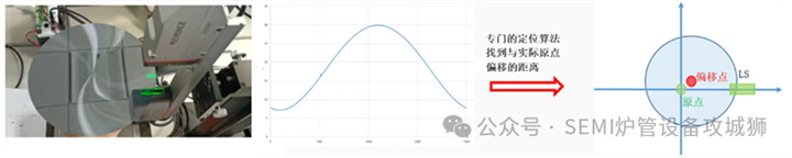
Optical edge finding systems typically include a light source, optical lens, and image sensor (such as CCD or CMOS). The light emitted by the light source shines on the surface of the wafer, and the edge of the wafer reflects the light. Focusing and imaging the reflected light with wafer edge information onto an image sensor through an optical lens. For a wafer, its edge is a continuous curve that appears as a contour with sudden changes in grayscale values in the image. Once the edge features are identified, the coordinates of the wafer edge in the image can be determined.
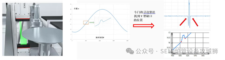
Wafer center positioning:
When the wafer rotates at the home bit of the chuck, the sensor calculates the x and y offset between the actual center and the chuck center by scanning the full circumference edge computing. Based on these offsets, drive the x/y-axis alignment platform to compensate for deviations and align the wafer center to the original chuck center.
(2)Mechanical Edge Searching
For aligners that cannot be calibrated using vacuum adsorption, the calibrator clamps the edge of the wafer and rotates it back and forth multiple times. Two sets of symmetrically arranged detection sensors detect the curvature of the wafer edge, calculate the center, cutting edge, and notch information of the wafer, and clamp CHUCK for center positioning calibration in the X and Y directions, and synchronously achieve angle correction.
5.summary
The EFEM (Equipment Front End Module), Load Port, Robot, and Aligner in semiconductor manufacturing equipment form the core system of wafer automation transfer, and the components work together to ensure high precision and efficiency in the manufacturing process. EFEM, as an "intelligent portal", provides clean environment and automated scheduling. Load Port enables precise docking of vehicles and wafer information management. Robot completes high-speed and high-precision wafer handling, while Aligner ensures precise wafer positioning. As the process evolves to 3nm and below, the system is showing three major development trends: precision requirements are moving from the micrometer level to the nanometer level (<10nm), and the level of intelligence is continuously enhanced through AI algorithms and digital twin technology. The technological breakthroughs in these key components directly determine the yield and production capacity of advanced processes, and are a key area of innovation in semiconductor equipment.