The invisible battlefield of chip packaging
In the field of semiconductor manufacturing, after the chip completes the pre-processing, it needs to be interconnected with the substrate or chip through bonding technology.
This technology is like the "soldering" of the chip world, directly determining the reliability, performance, and size of the chip. As Moore's Law approaches its physical limit, traditional packaging technology is facing severe challenges.
As the chip manufacturing process enters below 5 nanometers, the path to improving performance by reducing transistor size becomes increasingly difficult. Emerging technologies such as artificial intelligence, 5G communication, and autonomous driving have raised higher requirements for chip performance. In this context, advanced bonding technology has become one of the key paths to continue Moore's Law.
“In the context of the physical limitations challenges faced by semiconductor manufacturing in the post Moore era, the continuation of Moore's Law through advanced packaging technology has become a key platform for industry breakthroughs. "This is how the forward-looking report of the International Conference on Electronic Packaging Technology 2025 (ICEPT 2025) describes the importance of bonding technology.
The Evolution Path of Bonding Technology
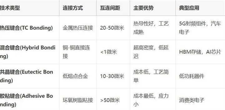
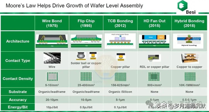
The semiconductor bonding process is mainly divided into three technical routes:
TC Bonding, as a representative of mature technology, creates a physical connection between two materials through heating and pressure. In high-pressure and high-temperature environments, material molecular chains are activated to form bonds, achieving electrical and thermal connections. Its core advantages lie in excellent thermal conductivity and high-density connectivity, making it suitable for high-performance computing, 5G communication, and other scenarios. But when faced with the demand for ultra-high density interconnection of AI chips, hot press bonding gradually reveals a side that is beyond its capabilities.
Hybrid Bonding, as a rising star in technological evolution, combines dielectric dielectric bonding with metal metal bonding to achieve vertical stacking between wafers or chips through direct copper to copper connections, without the need for traditional solder or bumps. This technology reduces the interconnect spacing to the level of 1 micron, with a density more than 10 times that of traditional technology.In 2025, storage giants such as Samsung and SK Hynix announced the introduction of hybrid bonding technology in HBM4, marking the transition of this technology from laboratory to mass production.
Other bonding techniques include Fusion Bonding, Hydrophilic Bonding, Eutectic Bonding, and Adhesive Bonding, each of which plays a role in different application scenarios.
Hybrid Bonding: The Revolution of Chip Interconnection
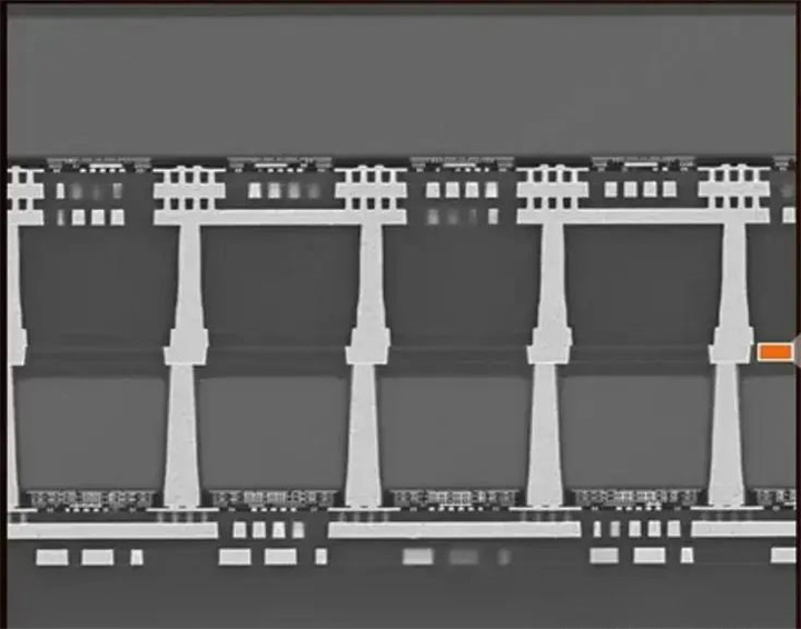
The core charm of hybrid bonding technology lies in its unique working principle. It achieves synchronous bonding between metals and oxides, as well as between oxides, through atomically flat contact surfaces, eliminating the size limitations and parasitic effects caused by traditional bump structures.
TSMC's SoIC (System on Integrated Chips) technology demonstrates the application value of hybrid bonding. As the industry's first high-density 3D chip stacking technology, SoIC-X adopts a hybrid bonding scheme, specifically targeting the needs of high-performance computing (HPC) and AI fields.
The production process of hybrid bonding is extremely precise:
1. Wafer Preparation
2. Oxide Deposition
3. Metal Deposition
4. Alignment and Bonding within ± 50 nanometers
5. Annealing
6. Inspection and Testing
Each step requires extremely high precision and environmental conditions, and any small deviation may affect the final bonding quality and chip performance.
The performance improvement brought by hybrid bonding is remarkable:
In logic chips, hybrid bonding increases interconnect density by 15 times, signal speed by 11.9 times, bandwidth density by 191 times, and energy consumption per bit by 20 times
In the field of High Bandwidth Memory (HBM), hybrid bonding reduces thermal resistance by 20%, dynamic power consumption by 17%, and signal integrity by 20%
The thickness of the bonding layer has been reduced from tens of micrometers to a few micrometers for micro bumps, providing the possibility of increasing the number of stacked layers while enhancing heat dissipation performance
Samsung Electronics executive Kim Dae woo admitted, "Even with a 16 layer stacked HBM, the heating problem is very difficult to control, so we are gradually trying to use hybrid bonding technology from this level
Application scenarios: From HBM to AI chips
In the field of storage chips, hybrid bonding technology is becoming a key solution to break through the bottleneck of traditional TSV technology. With the development of HBM towards higher stacking layers, hybrid bonding has successfully solved the problems of low heat dissipation efficiency and limited stacking height faced by traditional TSV+bump bonding through direct connection without convex points. SK Hynix has confirmed that this technology can achieve stacking of more than 20 layers with a thickness not exceeding 775 microns. In the field of 3D NAND, Yangtze Memory's Xtacking technology has taken the lead in achieving mixed bonding mass production. By separating and manufacturing peripheral circuits and integrating storage units, the I/O speed of NAND has been increased to 3.0Gbps. Its technical strength has been internationally recognized, and Samsung obtained its patent authorization for the next generation of products in February 2025.
Hybrid bonding technology is reshaping the chip architecture in the fields of AI chips and high-performance computing. This technology supports two integration methods, wafer level (W2W) and die level (D2W), and can interconnect heterogeneous components such as logic chips, memory chips, and AI accelerators with ultra-fine spacing of less than 10 nanometers, achieving more than 10 times the data transmission bandwidth improvement compared to traditional packaging. Intel and AMD have applied this technology to 3D V-Cache stacked processors, while Nvidia also plans to use hybrid bonded HBM5 memory in its next-generation AI GPU to meet the urgent demand for high bandwidth memory in AI computing.
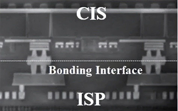
In the field of image sensors, hybrid bonding technology effectively reduces optical path loss and significantly reduces module size by directly connecting through silicon via (TSV) and copper, and has become a standard technology for high-end smartphone cameras. Sony has successfully achieved the separation of pixel units and signal processing units in CMOS image sensors through hybrid bonding technology, which not only improves imaging quality but also optimizes sensor performance. This innovative application demonstrates the unique advantages of hybrid bonding in improving the performance of optical devices.
Hybrid bonding technology is rapidly expanding from the initial storage chip field to more application scenarios. With the development of emerging technologies such as 5G communication, autonomous driving, and the Internet of Things, the demand for high-performance and low-power chips will continue to grow, which will open up broader application space for hybrid bonding technology. Especially in scenarios requiring high-density integration, such as edge computing devices and wearable devices, hybrid bonding technology is expected to become a key technology path to achieve chip miniaturization and performance improvement.
Technological Challenges and Global Racing
1. Process complexity and precision control challenges
The primary technical challenge faced by hybrid bonding lies in sub micron (<1 μ m) precision control, which requires precise alignment and bonding of billions of connection points. This process imposes almost stringent requirements on the cleanroom environment (requiring ISO level 3), material uniformity, and yield control. Even particle pollutants or organic residues at the 10nm level can lead to bonding interface defects, significantly reducing bonding strength. In addition, wafer to wafer (W2W) and chip to wafer (D2W) processes each have their own challenges: W2W requires extremely high global alignment accuracy, while D2W needs to address new challenges such as processing time per wafer (several hours) and maintaining hydrophilicity.
2. Cost and obstacles to mass production
Hybrid bonding technology is facing enormous cost pressure. The investment in a single wafer level bonding equipment exceeds 20 million US dollars, and the initial yield rate is usually only 60-70%. Currently, only a few companies in the world, such as TSMC and Applied Materials, have mature mass production capabilities, making it difficult for small and medium-sized manufacturers to bear the high cost of technology introduction. In addition, bonding failure can lead to the scrapping of twin circles, further increasing production costs, which has become an important obstacle to the popularization of technology.
3. The global competitive landscape presents a hierarchical differentiation
International semiconductor giants have formed a clear technological echelon:
Leading manufacturer: TSMC's SoIC technology has achieved mass production with a spacing of less than 1 μ m, leading the high-end market; Intel Foveros and Samsung HBM hybrid bonding technology have also entered the mass production stage
Equipment suppliers: ASML, Applied Materials, and Austrian EVG monopolize the key equipment market, among which EVG's magnetron plasma bonding equipment has an accuracy of ± 0.5 μ m
The Rise of Chinese Power: Tuojing Technology launches mass-produced W2W equipment "Dione 300", Qinghe Jingyuan releases the world's first C2W&W2W dual-mode equipment, and Maiwei Corporation achieves ± 100nm accuracy
4. Market prospects and technological innovation
Despite facing challenges, the market prospects for hybrid bonding devices are vast. According to Besi's prediction, the market demand will reach 2.8 billion euros by 2030, with a demand for over 1400 devices. Technological innovation is continuously breaking through bottlenecks:
The low-temperature hybrid bonding technology (<200 ° C) developed by Harbin Institute of Technology has solved the bonding problem of heat sensitive chips
The atomic level interface control scheme of the Institute of Microelectronics, Chinese Academy of Sciences has increased the yield to 99.9%
The research and development of new detection technologies and self-assembled materials are overcoming the challenge of nanoscale defect detection
5. Development trends under geopolitical influence
The US technology restrictions on China have accelerated the regionalization of the global hybrid bonding technology ecosystem. Chinese manufacturers are seeking breakthroughs through independent innovation and industrial chain collaboration, with Huawei investing in equipment manufacturers and Changdian Technology accelerating research and development. In the future, a tripartite technological landscape may emerge between China, the United States, and Europe, and hybrid bonding technology will continue to develop towards smaller spacing and higher stacking layers, becoming one of the core technologies for semiconductor manufacturing in the post Moore era.
Development prospects of hybrid bonding
1. Market Expansion: Penetrating from High end Chips to Consumer Electronics
Hybrid bonding technology is extending from high-end fields such as AI and HPC to consumer markets such as smartphones and automotive electronics. With the popularity of HBM5 and Chiplet architecture, as well as the growing demand for high bandwidth and low power consumption in autonomous driving chips, it is expected that the compound annual growth rate (CAGR) of the market size will exceed 30% from 2025 to 2030. Giants such as TSMC and Intel have included it in their mass production routes, while consumer electronics manufacturers such as Apple and Qualcomm are also evaluating the cost-effectiveness of this technology, which may drive larger scale applications in the future.
2. Process Innovation: Key Breakthrough in Low Temperature Bond Synthesis
Traditional hybrid bonding requires high-temperature annealing (>300 ° C), which can easily lead to chip warping and reliability issues. The low-temperature hybrid bonding technology (<200 ° C) developed by Wang Chenxi's team at Harbin Institute of Technology significantly reduces thermal stress, especially suitable for heat sensitive scenarios such as HBM storage stacking. Dr. Jin Renxi's atomic level surface and interface control scheme (Ra<1nm) from the Institute of Microelectronics, Chinese Academy of Sciences has further increased the bonding yield to 99.9%, solving the industry pain points of interface voids and insufficient mechanical strength, paving the way for mass production.
3. Technology driven: HBM and AI chip demand explosion
HBM5 and next-generation AI chips (such as NVIDIA Blackwell architecture) require higher density vertical interconnects, and hybrid bonding synthesis is a key technology for achieving 3D stacking. As the interconnect spacing moves towards sub micron (<1 µ m) and the number of chip stacking layers exceeds 20, traditional TSV and micro bump technologies are approaching their physical limits, and hybrid bonding will become the core means of improving performance in the post Moore's era.
4. Geopolitical impact: Accelerated regionalization of supply chains
The US restrictions on HBM related technologies in China may slow down the spread of hybrid bonding in China, but it also promotes independent innovation in the local industrial chain. Companies such as Changdian Technology and Tongfu Microelectronics are accelerating their research and development efforts, while Huawei Hubble is investing in equipment manufacturers to reduce dependence on international suppliers such as ASML and EVG. In the future, a mixed bonding technology ecosystem with a tripartite balance between China, the United States, and Europe may be formed.
5. Future outlook: Reshaping the semiconductor manufacturing landscape
Hybrid bonding is not only a technological innovation, but also a revolution in the integration of storage and logic chips. As 3D IC design becomes mainstream, this technology will be deeply integrated into Chiplet architecture, becoming a new engine for improving semiconductor performance. Although challenges such as nanoscale defect detection and equipment costs still exist, technological advancements such as self-assembled materials and new detection methods are continuously breaking through bottlenecks. By 2030, hybrid bonding is expected to become the standard solution for advanced packaging, completely changing the boundaries of chip manufacturing.