
HBM Overview
HBM (High Bandwidth Memory) is an innovative 3D stacked DRAM technology jointly developed by AMD and SK hynix. This technology provides bandwidth and capacity far beyond traditional DRAM by vertically stacking multiple layers of DRAM chips and utilizing high bandwidth serial interfaces to achieve direct connection with GPUs or CPUs. High bandwidth memory (HBM) symbolizes a revolutionary leap in memory technology, especially in fields such as high-performance computing (HPC), artificial intelligence (AI), data centers, and high-end gaming.
Memory Evolution History
The development of memory technology from early static random access memory (SRAM) and dynamic random access memory (DRAM) has gone through multiple key stages:
The birth of SRAM and DRAM: SRAM is suitable for caching scenarios due to its high-speed access characteristics, while DRAM has become the preferred main memory due to its high storage density and cost-effectiveness.
Synchronous Dynamic Random Access Memory (SDRAM): Introduced to narrow the speed gap between memory and CPU, it enables data read and write within a single clock cycle.
Double Data Rate Synchronous Dynamic Random Access Memory (DDR SDRAM): uses clock rising and falling edges to transfer data, doubling the data transfer rate.
The development of multi data rate technology: from DDR to DDR2, DDR3, DDR4 to DDR5, the memory data transfer rate continues to increase, and power consumption and cost-effectiveness are constantly optimized.
HBM principle
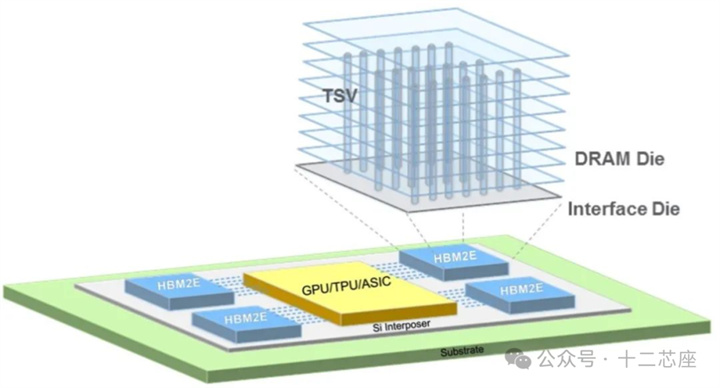
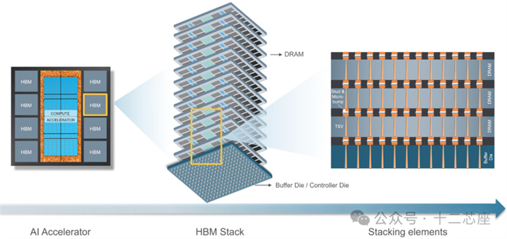
The core of HBM lies in its unique 3D stacking architecture and TSV (Through Silicon Via) technology:
3D Stacking Architecture: Vertically stacking multiple DRAM chip layers to increase memory capacity per unit area, with each layer of DRAM connected to the logic chip through micro bumps.
TSV technology: Vertically penetrating conductive paths in silicon chips to connect circuits at different levels, reducing the length and resistance of inter chip connections.
High bandwidth serial interface: Compared with traditional parallel interfaces, serial interfaces achieve higher data transmission rates with fewer pins.
HBM Advantage
High bandwidth: meets high-performance computing needs, with bandwidth far exceeding traditional DRAM.
High capacity: 3D stacking technology integrates more DRAM layers within the same chip area, providing greater memory capacity.
Low power consumption: Vertical stacking structure reduces data transmission distance, and TSV technology also helps to reduce power consumption.
Small size: The 3D stacking design significantly reduces the size of the memory module, which is conducive to compact system design.
Development history of HMB technology
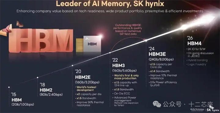
In 2013:
AMD and SK hynix announced a collaboration to develop HBM technology.
In 2015:
The beginning of HBM technology had a bandwidth of 1.0Gbps and a capacity of 2Gb.
In 2018:
Capacity increased to 8Gb, bandwidth increased to 2.4Gbps. It is the fastest developing version in the world, with a doubled capacity per chip, a 1.5-fold increase in bandwidth, and a 34% increase in thermal resistance compared to its predecessor.
In 2020:
The capacity and bandwidth reach 16Gb and 3.2Gbps. It has significantly increased in both speed and capacity.
In 2022:
The bandwidth has been increased to 5.6Gbps, and SK Hynix has achieved global mass production for the first time. This technology has a 1.5-fold capacity increase, a 1.8-fold bandwidth increase, a 1.2Hi connection, and also utilizes on-chip chip (On Die) and advanced power management (via Temp. management) technologies.
In 2024:
The capacity reaches 24Gb and the bandwidth is as high as 8.0Gbps. The capacity of each chip has increased by 1.5 times, the bandwidth has increased by 1.4 times, and the thermal resistance has been improved by 10%. The energy efficiency has reached 0.9x (pJ/bit).
In 2026:
We plan to launch HBM4 technology in 2026, which will be discussed under JEDEC standards, using hybrid bonding technology and logic wafer fab production.
summarize
High bandwidth memory (HBM), as a revolutionary technology in modern computing, has achieved comprehensive breakthroughs in performance, capacity, power consumption, and size with its unique 3D stacking architecture and TSV technology. Since its launch in 2013, HBM has undergone multiple iterative upgrades, from an initial bandwidth of 1.0Gbps to the current 8.0Gbps, which has not only driven rapid development in high-performance computing, artificial intelligence, data centers, and other fields, but also laid a solid foundation for future technological evolution. Looking ahead to the future, with the gradual implementation of HBM4 technology, this technology will continue to lead the trend of memory development and inject stronger impetus into the intelligent process of human society.