
1、What is WLCSP?
WLCSP (Wafer Level Chip Scale Package) is an advanced integrated circuit packaging technology, characterized by direct packaging on the wafer, with a final packaging size close to the size of the chip itself. This technology achieves high-density interconnection and miniaturized packaging by rewiring and bump manufacturing on the wafer, and is widely used in the fields of mobile devices, consumer electronics, and high-performance computing.
2、What is the classification of WLCSP?
Fan In wafer level chip packaging (WLCSP): The pins are led out from around the chip and introduced into the bottom of the chip in a fan-shaped manner. It has the characteristics of small size, low cost, and good heat dissipation, but the number of pins is relatively small, making it impossible to achieve high integration chip packaging.
Fan Out wafer level chip packaging (WLCSP): The pins are led out from the bottom of the chip in a fan-shaped manner to the outside of the chip. With a large number of pins and flexible circuit design, it can package multiple chips into one, achieving higher integration while meeting small size requirements.
3、WLCSP Process Flow
1. Wafer preparation
Wafer cleaning: Removing surface particles, organic matter, and metal residues.
Surface treatment: Improving the adhesion performance of wafer surface through chemical or physical methods.
2.Passivation layer deposition
Deposit a layer of passivation material (such as SiO ₂ or SiN) on the surface of the wafer to protect internal circuits and provide insulation. Common method: PECVD (Plasma Enhanced Chemical Vapor Deposition).
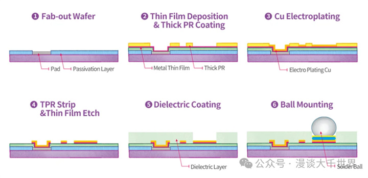
3. Solder pad window
Use photolithography technology to open windows on the passivation layer, exposing aluminum pads. Accurate patterning is achieved through wet etching or dry etching.
4. Redistribution Layer (RDL)
Create a rewiring layer on the surface of the wafer to rearrange the originally scattered small pads into a larger pad array. The steps are as follows: first, deposit conductive materials (such as copper or aluminum), then etch to form the desired wiring pattern, and finally, perform surface passivation treatment.
5.Under Bump Metallurgy (UBM)
Deposit one or more layers of metal thin films on the surface of the rewiring layer's solder pads to improve the adhesion and conductivity between the solder balls and the solder pads. Common materials: Ti/Cu/Ni/Au.
6. Welding ball planting ball
Place solder balls (such as SnAgCu alloy solder balls) on the solder pads of the rewiring layer. Solder balls can be fixed by printing, electroplating, or reflow soldering.
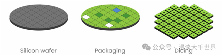
7. wafer sawing
Use laser cutting or cutting machines to divide the packaged wafer into individual chips. Please ensure that the cutting path does not damage the functionality of the chip.
8. Finished product testing
Perform electrical performance testing and visual inspection on individual chips after cutting. The test content includes conductivity, insulation, solder ball position deviation, etc.
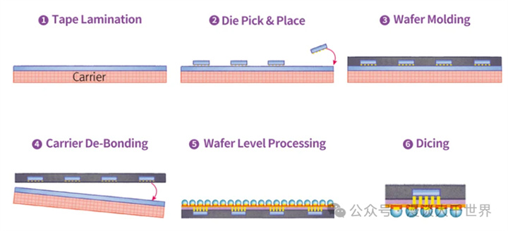
9. Final packaging
Load qualified chips into the final packaging carrier (such as plastic packaging or glass substrate). Perform sealing treatment to prevent external environmental influences.